- 您现在的位置:买卖IC网 > Sheet目录369 > W948D2FBJX5E (Winbond Electronics)IC LPDDR SDRAM 256MBIT 90VFBGA
�� �
�
�W948D6FB� /� W948D2FB�
�256Mb� Mobile� LPDDR�
�19.� tHZ� and� tLZ� transitions� occur� in� the� same� access� time� windows� as� valid� data� transitions.� These� parameters�
�are� not� referred� to� a� specific� voltage� level,� but� specify� when� the� device� is� no� longer� driving� (HZ),� or� begins�
�driving� (LZ).�
�20.� tDQSQ� consists� of� data� pin� skew� and� output� pattern� effects,� and� p-channel� to� n-channel� variation� of� the� output�
�drivers� for� any� given� cycle.�
�21.� The� specific� requirement� is� that� DQS� be� valid� (HIGH,� LOW,� or� some� point� on� a� valid� transition)� on� or� before�
�the� corresponding� CK� edge.� A� valid� transition� is� defined� as� monotonic� and� meeting� the� input� slew� rate�
�specifications� of� the� device.� When� no� writes� were� previously� in� progress� on� the� bus,� DQS� will� be� transitioning�
�from� Hi-Z� to� logic� LOW.� If� a� previous� write� was� in� progress,� DQS� could� be� HIGH,� LOW,� or� transitioning� from�
�HIGH� to� LOW� at� this� time,� depending� on� tDQSS.�
�22.� The� maximum� limit� for� this� parameter� is� not� a� device� limit.� The� device� operates� with� a� greater� value� for� this�
�parameter,� but� system� performance� (bus� turnaround)� will� degrade� accordingly.�
�23.� A� low� level� on� DQS� may� be� maintained� during� High-Z� states� (DQS� drivers� disabled)� by� adding� a� weak� pull-�
�down� element� in� the� system.� It� is� recommended� to� turn� off� the� weak� pull-down� element� during� read� and� write�
�bursts� (DQS� drivers� enabled).�
�24.� At� least� one� clock� cycle� is� required� during� tWR� time� when� in� auto� precharge� mode.�
�25.� tDAL� =� (tWR/tCK)� +� (tRP/tCK):� for� each� of� the� terms,� if� not� already� an� integer,� round� to� the� next� higher� integer.�
�26.� There� must� be� at� least� two� clock� pulses� during� the� tXSR� period.�
�27.� There� must� be� at� least� one� clock� pulse� during� the� tXP� period.�
�28.� tREFI� values� are� dependence� on� density� and� bus� width.�
�29.� A� maximum� of� 8� Refresh� commands� can� be� posted� to� any� given� M,� meaning� that� the� maximum� absolute�
�interval� between� any� Refresh� command� and� the� next� Refresh� command� is� 8*tREFI.�
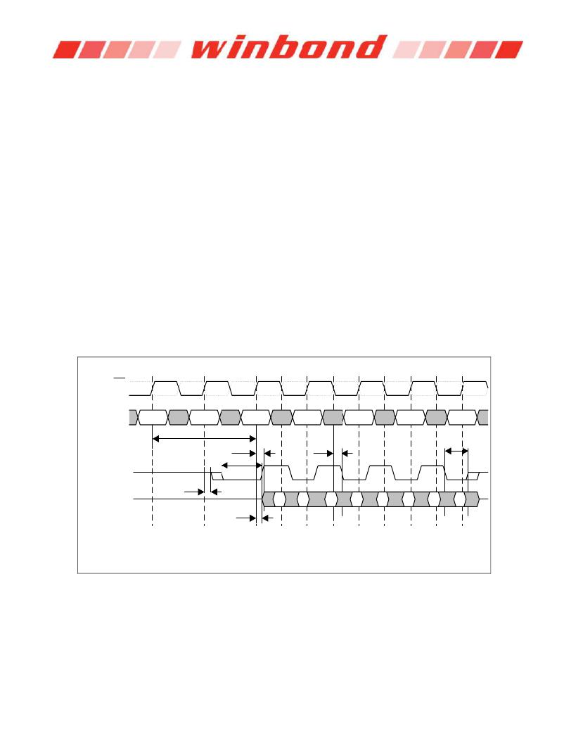
�8.5.1� CAS� Latency� Definition� (With� CL=3)�
�T0�
�T1�
�T2�
�T2n�
�T3�
�T3n�
�T4�
�T4n�
�T5�
�T5n�
�T6�
�CK�
�CK�
�Command�
�READ�
�NOP�
�NOP�
�NOP�
�NOP�
�NOP�
�NOP�
�DQS�
�CL=3�
�t� DQSCKmin�
�t� RPRE�
�t� DQSCKmin�
�t� RPST�
�All� DQ,�
�collectively�
�t� LZmin�
�t� LZmin�
�T2�
�T2n�
�T3�
�T3n�
�T4�
�T4n�
�T5�
�T5n�
�1)DQ� transitioning� after� DQS� transition� define� tDQSQ� window.�
�2)ALL� DQ� must� transition� by� tDQSQ� after� DQS� transitions,� regardless� of� tAC�
�3)tAC� is� the� DQ� output� window� relative� to� CK,and� is� the� long� term� component� of� DQ� skew.�
�Publication� Release� Date� :� Oct,� 15,� 2012�
�-� 54� -�
�Revision� :� A01-004�
�发布紧急采购,3分钟左右您将得到回复。
相关PDF资料
W949D2CBJX5E
IC LPDDR SDRAM 512MBIT 90VFBGA
W971GG6JB25I
IC DDR2 SDRAM 1GBIT 84WBGA
W971GG8JB-25
IC DDR2 SDRAM 1GBIT 60WBGA
W9725G6IB-25
IC DDR2-800 SDRAM 256MB 84-WBGA
W9725G6JB25I
IC DDR2 SDRAM 256MBIT 84WBGA
W9725G6KB-25I
IC DDR2 SDRAM 256MBIT 84WBGA
W972GG6JB-3I
IC DDR2 SDRAM 2GBITS 84WBGA
W9751G6IB-25
IC DDR2-800 SDRAM 512MB 84-WBGA
相关代理商/技术参数
W948D2FBJX5ETR
制造商:Winbond Electronics Corp 功能描述:256M MDDR, X32, 200MHZ
W948D2FBJX5I
制造商:Winbond Electronics Corp 功能描述:DRAM Chip DDR SDRAM 256M-Bit 8Mx32 1.8V 90-Pin VFBGA 制造商:Winbond Electronics Corp 功能描述:IC MEMORY
W948D2FBJX5I TR
制造商:Winbond Electronics Corp 功能描述:256M MDDR, X32, 200MHZ, INDUST
W948D2FBJX6E
制造商:Winbond Electronics Corp 功能描述:DRAM Chip DDR SDRAM 256M-Bit 8Mx32 1.8V 90-Pin VFBGA 制造商:Winbond Electronics 功能描述:LOW POWER DRAM 制造商:Winbond Electronics Corp 功能描述:IC MEMORY
W948D2FBJX6ETR
制造商:Winbond Electronics Corp 功能描述:256M MDDR, X32, 166MHZ, 65NM
W948D2FBJX6G
制造商:WINBOND 制造商全称:Winbond 功能描述:256Mb Mobile LPDDR
W948D6FB
制造商:WINBOND 制造商全称:Winbond 功能描述:256Mb Mobile LPDDR
W948D6FBHX5E
功能描述:IC LPDDR SDRAM 256MBIT 60VFBGA RoHS:是 类别:集成电路 (IC) >> 存储器 系列:- 标准包装:1 系列:- 格式 - 存储器:闪存 存储器类型:闪存 - NAND 存储容量:4G(256M x 16) 速度:- 接口:并联 电源电压:2.7 V ~ 3.6 V 工作温度:0°C ~ 70°C 封装/外壳:48-TFSOP(0.724",18.40mm 宽) 供应商设备封装:48-TSOP I 包装:Digi-Reel® 其它名称:557-1461-6